MIT scientists establish approach to develop nanoLEDs for XR make use of Headlines about virtual reality
July 11, 2023– Researchers at Massachusetts Institute of Modern Technology (MIT) have actually cultivated a brand new approach for integrating halide perovskite nanocrystals right into nanoscale tools. The procedure permits the specific development of nanoscale LEDs (nanoLEDs), which can have potential applications in augmented and also virtual fact (AR/VR) shows.
Halide perovskites are actually a group of components known for their remarkable optoelectronic residential properties, creating them best for high-performance solar cells, laser devices, and light-emitting diodes (LEDs).
Previously, incorporating these products at the nanoscale has actually been actually testing as a result of their fragile attribute and sensitivity to harm during the course of typical manufacture methods. To eliminate this difficulty, MIT analysts devised a method that allows exact on-site development of individual halide perovskite nanocrystals, along with control over their location within fifty nanometers (a sheet of newspaper is actually 100,000 nanometers heavy).
According to MIT, the impressive brand new technique makes it possible for not simply accurate control over the nanocrystals’ positioning yet also allows for exact command over their dimension, which straight affects their qualities as well as performance. Through growing the material regionally along with intended features, the necessity for conventional lithographic pattern steps that might possibly trigger damages is gotten rid of.
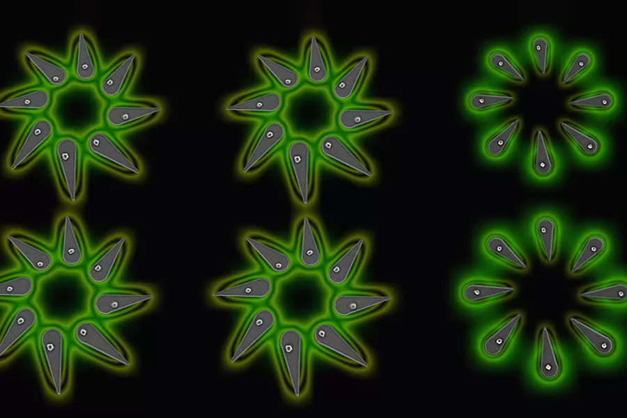
MIT noted that the approach is scalable, versatile, and also suitable along with standard fabrication actions, making it ideal for including nanocrystals in to useful nanoscale units. Scientist effectively took advantage of the strategy to produce varieties of nanoscale LEDs (nanoLEDs), which shine when electrically activated. These arrays possess possible treatments in optical communication as well as computer, lensless microscopic lens, quantum light sources, and also high-density, high-resolution screens for enhanced and online reality.
The researchers’ method involved creating a nanoscale template with little wells which contain the chemical process through which crystals increase. By tweaking the template’s surface area and the inside of the wells, analysts had the capacity to regulate a building called “wettability,” guaranteeing that the service consisting of the perovskite material continues to be restricted within the wells.
The design of these wells participates in an important job in identifying the nanocrystal positioning. By altering the well’s shape, researchers managed to craft nanoscale troops that make it possible for advantageous placement of the crystals at intended areas. Additionally, they found out that they can accurately handle the dimension of the crystals through readjusting the dimension of the wells.
“As our work reveals, it is critical to develop brand-new engineering frameworks for integration of nanomaterials right into useful nanodevices. By moving past the conventional perimeters of nanofabrication, materials design, and also tool style, these methods can permit our company to use matter at the excessive nanoscale sizes, assisting us recognize unique device systems vital to taking care of surfacing technical necessities,” pointed out Farnaz Niroui, the EE Landsman Job Growth Assistant Lecturer of Electrical Design as well as Computer Science (EECS), a participant of the Lab of Electronic Devices (RLE), and senior author of a brand new report that defines the job.
The research study results were actually released in Nature Communications, with the interdisciplinary effort involving scientists from electric design, information technology, and chemical design. The work was assisted, in part, due to the National Scientific Research Groundwork as well as the MIT Facility for Quantum Design.
MIT stated that the investigation staff prepares to discover more treatments for these small lights and also test excess of miniaturization so as to successfully integrate all of them in to quantum bodies. Beyond nanoscale source of lights, the procedure likewise opens other options for establishing halide perovskite-based on-chip nanodevices, according to MIT.
For the total message on the study statement, click on this link.
Photo credit: MIT
Sam Sprigg
Sam is the Owner and also Handling Publisher of Auganix. Along with a history in study as well as document writing, he has been covering XR industry information for the past 5 years.